 .pdf
.pdf
RED: floating-gate nMOS transistor
This example shows the distribution of the electric potential \(V\) in a nanoscale floating-gate nMOS (Metal-Oxide-Semiconductor) transistor working in inversion conditions. The prefix "n" indicates that the electric current is due to negatively charged electrons. This simulation involves a non-homogeneous problem with internal interfaces and it has been solved with the HDG method applied to the Darcy problem. A more detailed description of this test case is illustrated in [HDG2018].
1. Running the case
The command line to run this case is
mpirun -np 4 feelpp_toolbox_mixed-poisson-model_3DP1 --case "github:{repo:toolbox,path:examples/modules/poisson/examples/red}"2. Data files
The case data files are available in Github here
3. Geometry
A scheme of a realistic floating-gate nMOS transistor used as a nonvolatile memory device is shown with the schematic representation of the two-dimensional cross-section in which the control gate is now included for sake of simplicity in the following Figure:
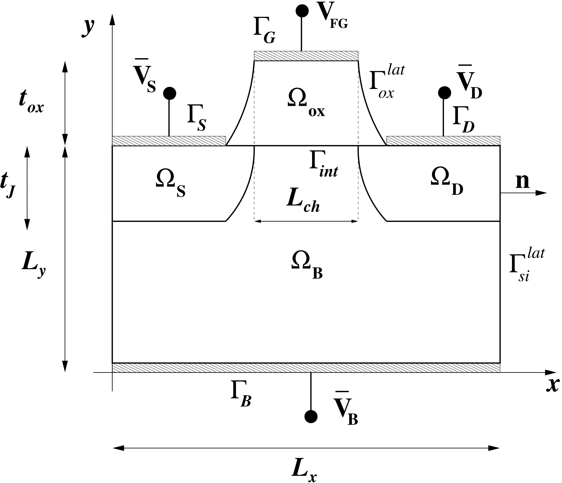
The device is composed of a pair of n-doped source and drain regions, a p-doped substrate region and a silicon dioxide (SiO2) region in which a control gate and a floating gate are buried. The floating gate is isolated from the control gate by an inter-polysilicon dielectric (IPD) layer beneath the control gate.
The geometry has been generated with GMSH:
h = 0.1;

Lx = DefineNumber[480*10^(-9), Name "x Lenght"];
Ly = DefineNumber[320*10^(-9), Name "y Lenght"];
Lz = DefineNumber[320*10^(-9), Name "z Lenght"];
Lj = DefineNumber[160*10^(-9), Name "j Lenght"];
t0x = DefineNumber[10*10^(-9), Name "Gate Length"];

// Discretization
npt = DefineNumber[20, Name "Nb point interp"];
l = DefineNumber[3.5, Name "Interv for tanh"];

A = newp; Point(A) = {0,0,0,h};
B = newp; Point(B) = {Lx,0,0,h};
C = newp; Point(C) = {Lx,Ly,0,h};
D = newp; Point(D) = {2./3.*Lx,Ly,0,h/3};
E = newp; Point(E) = {2./3.*Lx-Lx/8.,Ly,0,h/3};
F = newp; Point(F) = {1./3.*Lx+Lx/8.,Ly,0,h/3};
G = newp; Point(G) = {1./3.*Lx,Ly,0,h/3};
H = newp; Point(H) = {0,Ly,0,h};
K = newp; Point(K) = {2./3.*Lx-Lx/8.,Ly+t0x,0,h/3};
L = newp; Point(L) = {1./3.*Lx+Lx/8.,Ly+t0x,0,h/3};
M = newp; Point(M) = {0,Ly-Lj,0,h};
N = newp; Point(N) = {1./3.*Lx,Ly-Lj,0,h};
P = newp; Point(P) = {Lx,Ly-Lj,0,h};
Q = newp; Point(Q) = {2./3.*Lx,Ly-Lj,0,h};

AB = newl; Line(AB) = {A,B};
BP = newl; Line(BP) = {B,P};
PC = newl; Line(PC) = {P,C};
CD = newl; Line(CD) = {C,D};
DE = newl; Line(DE) = {D,E};
EF = newl; Line(EF) = {E,F};
FG = newl; Line(FG) = {F,G};
KL = newl; Line(KL) = {K,L};
GH = newl; Line(GH) = {G,H};
HM = newl; Line(HM) = {H,M};
MA = newl; Line(MA) = {M,A};
MN = newl; Line(MN) = {M,N};
PQ = newl; Line(PQ) = {P,Q};

pListNF[0] = N;
pListQE[0] = Q;
pListGL[0] = G;
pListDK[0] = D;
For i In {1:npt-1}
    xhi = i*Lx/8./npt;
    eta = 64*Lj/(Lx*Lx)*xhi*xhi;
    xNF = 1./3.*Lx + xhi;
    xQE = 2./3.*Lx - xhi;
    y = eta + Ly - Lj;
    pListNF[i] = newp;
    Point(pListNF[i]) = {xNF,y,0,h};
    pListQE[i] = newp;
    Point(pListQE[i]) = {xQE,y,0,h};
    eta = t0x/2.*(Tanh(16.*l/Lx*xhi-l)+1);
    xGL = xNF;
    xDK = xQE;
    y = Ly + eta;
    pListGL[i] = newp;
    Point(pListGL[i]) = {xGL,y,0,h/3};
    pListDK[i] = newp;
    Point(pListDK[i]) = {xDK,y,0,h/3};
EndFor
pListNF[npt] = F;
pListQE[npt] = E;
pListGL[npt] = L;
pListDK[npt] = K;

NF = newl; Spline(NF) = pListNF[];
QE = newl; Spline(QE) = pListQE[];
GL = newl; Spline(GL) = pListGL[];
DK = newl; Spline(DK) = pListDK[];

Bll = newll; Line Loop(Bll) = {AB,BP,PQ,QE,EF,-NF,-MN,MA};
OB = news; Plane Surface(OB) = {Bll};

Dll = newll; Line Loop(Dll) = {PC,CD,DE,-QE,-PQ};
OD = news; Plane Surface(OD) = {Dll};

Sll = newll; Line Loop(Sll) = {FG,GH,HM,MN,NF};
OS = news; Plane Surface(OS) = {Sll};

Gll = newll; Line Loop(Gll) = {DE,EF,FG,GL,-KL,-DK};
OG = news; Plane Surface(OG) = {Gll};

// 3D
out[] = Extrude{0,0,Lz} {Surface{OB,OD,OS,OG};};

// For i In {0:#out[]-1}
//     Printf("out[%g] : %g",i, out[i]);
// EndFor

Physical Surface("Bulk") = {out[2]};
Physical Surface("Drain") = {out[13]};
Physical Surface("Source") = {out[20]};
Physical Surface("Gate") = {out[30]};
Physical Surface("IntBD") = {out[4],out[5]};
Physical Surface("IntBG") = {out[6]};
Physical Surface("IntBS") = {out[7],out[8]};
Physical Surface("IntDG") = {out[14]};
Physical Surface("IntSG") = {out[19]};
Physical Surface("WallB") = {OB,out[0],out[3],out[9]};
Physical Surface("WallD") = {OD,out[10],out[12]};
Physical Surface("WallS") = {OS,out[17],out[21]};
Physical Surface("WallG") = {OG,out[24],out[29],out[31]};

Physical Volume("OmegaB") = {out[1]};
Physical Volume("OmegaD") = {out[11]};
Physical Volume("OmegaS") = {out[18]};
Physical Volume("OmegaG") = {out[25]};
N.B.: the unit of measure used in the .geo file are in mm.
4. Input parameters
Physical parameters:
| Name | Symbol | Value | Unit | |
|---|---|---|---|---|
electron charge |
\(q\) |
1.602e-19 |
\(C\) |
|
permittivity of vacuum |
\(\varepsilon_0\) |
8.854e-12 |
\(F \: m^{-1}\) |
|
relative permittivity of silicon |
\(\varepsilon^{si}_r\) |
11.7 |
stem:[ - ] |
|
relative permittivity of silicon dioxide |
\(\varepsilon^{ox}_r\) |
3.9 |
stem:[ - ] |
|
thermal voltage (at 300K) |
\(V_{th}\) |
0.02589 |
\(V\) |
|
intrinsic concentration (at 300K) |
\(n_i\) |
1.45e16 |
\(m^{-3}\) |
Device parameters:
| Name | Symbol | Value | Unit | |
|---|---|---|---|---|
horizontal length |
\(L_x\) |
480e-9 |
\(m\) |
|
vertical length |
\(L_y\) |
320e-9 |
\(m\) |
|
width |
\(L_z\) |
320e-9 |
\(m\) |
|
oxide thickness |
\(t_{ox}\) |
10e-9 |
\(m\) |
|
source and drain lengths |
\( \lvert \Gamma_S \rvert, \lvert \Gamma_D \rvert \) |
160e-9 |
\(m\) |
|
channel length |
\(L_{ch}\) |
40e-9 |
\(m\) |
|
junction depth |
\(t_J\) |
106e-9 |
\(m\) |
|
source potential |
\(\bar{V}_S \) |
0 |
\(V\) |
|
bulk potential |
\(\bar{V}_B \) |
0 |
\(V\) |
|
drain potential |
\(\bar{V}_D\) |
0 |
\(V\) |
|
source doping concentration |
\(\bar{N}_S\) |
1e26 |
\(m^{-3}\) |
|
bulk doping concentration |
\(\bar{N}_B\) |
5e22 |
\(m^{-3}\) |
|
drain doping concentration |
\(\bar{N}_D\) |
1e26 |
\(m^{-3}\) |
5. Model & Toolbox
-
The main goal of the simulations is to determine, via the integral boundary condition, the value attained on \(\Gamma_G\) at inversion conditions by the electric potential. This value is the threshold voltage of the device, denoted henceforth by \(V_T\) , and is a fundamental design parameter in integrated circuit nanoelectronics. The accurate prediction of the threshold voltage may be significantly influenced by the numerical treatment of the heterogeneous material device structure across the interface \(\Gamma_{int}\). With this respect the HDG framework appears to be the ideal computational approach because it allows to enforce, at the same time and in a strong manner, (a) the jump of the normal component of the electric displacement vector across the interface and (b) the continuity of the electric potential, at suitable quadrature nodes on each face belonging to \(\Gamma_{int}\), unlike standard displacement-based finite element discretization schemes which satisfy property (b) but fail at satisfying property (a).
-
Config file:
directory=toolboxes/hdg/mixed-poisson/red

[picard]
itol=1e-15
itmax=5

[exporter]
element-spaces=P0

[gmsh]
filename=$cfgdir/new_red.geo
hsize=5e-5

[mixedpoisson]
// pc-type=gasm
// sub-pc-factor-mat-solver-package-type=umfpack
// sub-pc-type=lu
ksp-monitor=1
ksp-rtol=1e-14
conductivity_json=k
filename=$cfgdir/new_red.json

[bdf]
order=1
[ts]
time-initial=0.0
time-step=10
time-final=150
steady=1 #false #true5.2. Boundary conditions
- Boundary conditions
- Interface conditions
The quantities \(\bar{V}|_{bi,j}\) are the built-in potentials associated with the subdomain regions \( \Omega_j ,\: j = S,D,B \), while \( \bar{N}_B \) is the concentration of ionized dopants in the bulk region and \(\delta\) is the width of the accumulation region in the \(y\) direction of the channel.
6. Outputs
6.1. Potential and current
Spatial distribution of the potential and direction of the current in the electronic device at steady state in inversion condition.
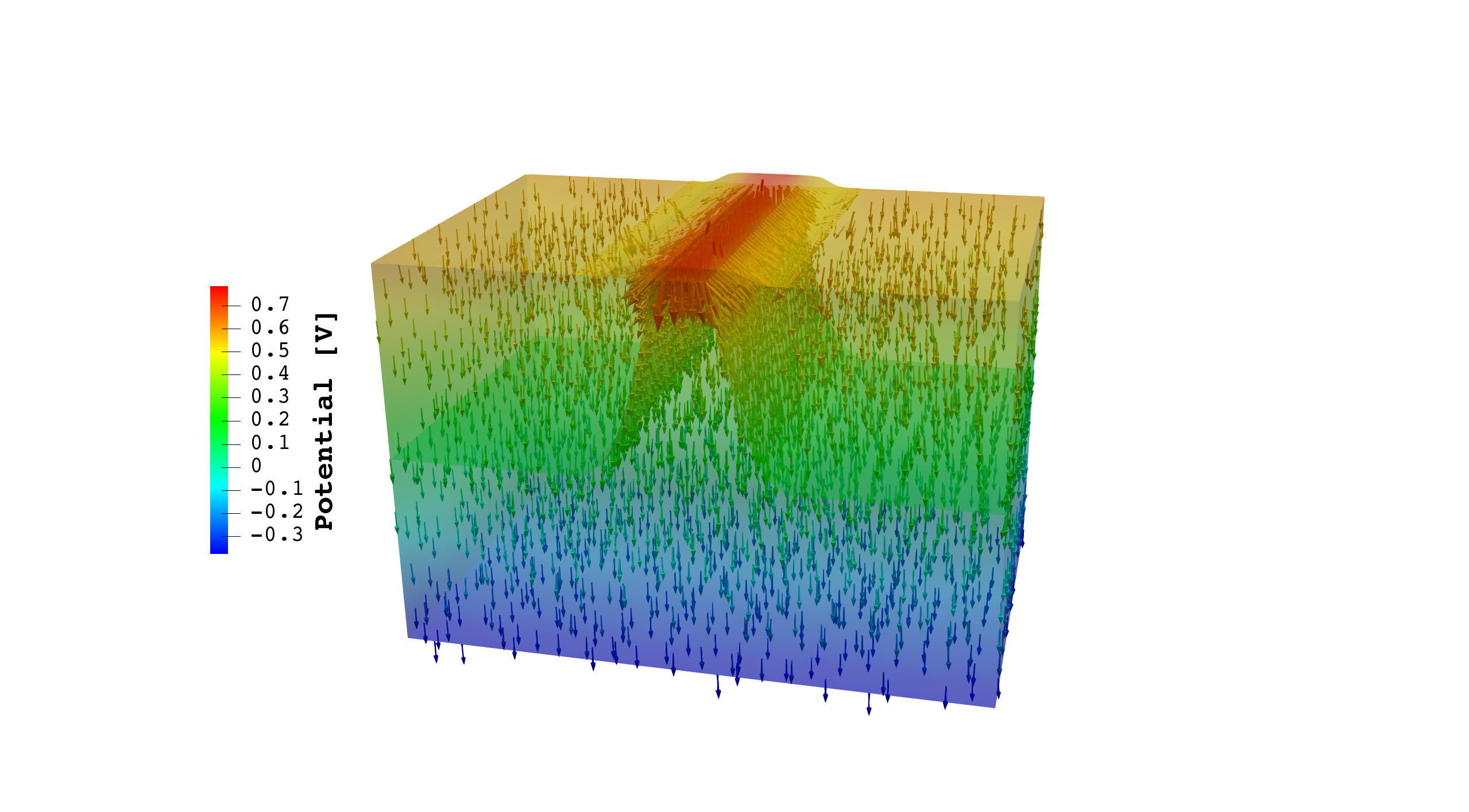
Spatial distribution of the electric field and its direction in the electronic device at steady state in inversion condition.
![]()
6.2. 3D model
In the window below, you can manipulate the 3D model at steady state.
| Click top left button on opengl window to change basic visualisation features |
6.3. Measures
The predicted value of \(V_T\) is positive and given by \(V^{computed}_T = 0.854926\) V.
The sign of \(V^{computed}_T\) is in physical agreement with the fact that the transistor is of n type, so that electron charges (negative) are attracted from the bulk region up towards the gate contact.
To quantitatively assess the accuracy of the estimate of the threshold voltage we adopt the analytical theory for an ideal MOS system developed in [Muller1986][Chapter 8] and use formula (8.3.18) of [Muller1986] to obtain \(V^{ideal}_T = 0.8591\) V, which agrees with the value predicted by the numerical simulation.